New Toy - The Sequel
Previously on DIY-HomeWorks: Plexus got a nice little prototyping board from his buddy. Little did he know that it would bring him a week full of wonder, excitement and tedious bug fixing.
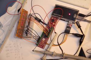
It was a drizzly Friday when I wrote the first article about that prototyping board. After a weekend worth of feature creep I ended up with this feature list:
- 16bit GPIO | Input: Hi-Z, Pull-Up | Output: Totem-Pole, Open-Drain | In/Out "LED Mode" with inline resistor (built-in)
- Separate high byte, low byte, word access | Burst output of up to 255 bytes/words
- Control via RS232 | protocol optimized for efficiency | default: 57600 BAUD 8N1 | Max: 230400 BAUD
- 2x Current DAC | 8 bit | DAC 2 can be buffered via internal OpAmp
- 2x ADC | 12 bit
- Edge triggered readout of IO
- Periodic readout of IO & ADC | 0.001 – 65 sec interval
- External triggered readout of IO & ADC
- Pulse generator | 15mHz – 500kHz | shortest pulse: 1µs
- ADC live monitoring
- Console access for easy manual control & monitoring
- Highly configurable
While this doesn't look too bad, it turned out to be quite the workload.
The Motivation
Once in while I need a simple 16bit GPIO module that I can easily control via good old RS232. Getting a decent 16bit PIO is hard enough on it's own, but getting one that brings a flexible RS232 interface can get pretty expensive pretty quickly. That's where that Module comes in. It's the CY8CKIT-043 an ARM Cortex PSoC 4200M Series Prototyping Kit from Cypress. (Update May 2022: Cypress was bought by Infineon, apparently. Links still work, though.)

Since I got it as a "here, have fun with it", and had no immediate use for it, I thought I implement my own 16bit GPIO module. I can always use it for something else later.
Unfortunately, I thought it would be a waste to ignore all the neat features of that controller. ADC, DAC, many timers, many different input and drive modes of the IO pins, programmable logic, … . So I added a lot of features to the thing. To the point where I think this could be useful for other people as well. But! Many of the peripheral modules of the controller can be configured in many different – useful – ways. So that screams for implementing an interface to make all those settings. Also, find a way to store some of them nonvolatile. And add someting to be able to read out that configuration. And document the whole shebang.
The goal was to have the interface as simple as possible but still easy to handle by hand. That meant no additional software should be necessary to work with the module. To prove my point in a pretty nerdy way, I hooked it up to a 25 year old VT100 terminal. Oh, do I love that font :D
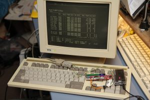
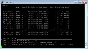
The terminal shows the short version of the status screen (command 'q', long version: [Space]). Above the status screen is the command I entered to get the low byte set to output, switch on the LED and show the status screen. The exclamation marks behind each command is the acknowledge character from the PIO. The USB hub is just the power supply.
How-To
In its simplest form it's just the Module as it is. You download and install the development environment, download and unpack the project files, plug in the PSoC-Board, 'Build' and 'Program', done. PIO ready to roll at 57600 BAUD 8N1.
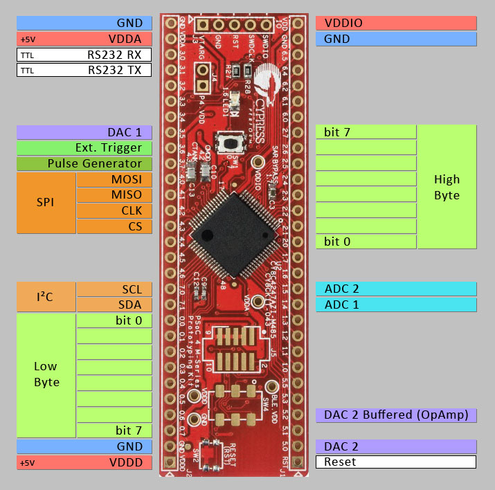
GPIO – Port 0 (Low Byte) & Port 2 (High Byte)
All pins can be configured individually. Either input(1) or output(0). If set to input, a pull-up resistor (~5k) can be switched on. The output can be either in a low impedance totem pole or open drain configuration. The low byte is on port 0, the high byte on port 2.
Due to the construction of the output stage of the controller, inputs with pull-ups must be held in a high state from a software point of view. So, all pins that are set to input are always set to high by the firmware. The last value that was sent to the port is cached so that pins are set to the right state when they're changed from inputs to outputs, this makes it possible to do stuff like Charlieplexing, where pins are set while they're still Hi-Z.
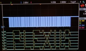
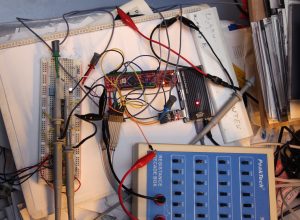
This was created by using the burst transfer function. That allows the the transmission of up to 255 bytes or words without having to send a command between the actual values.
For example, the command to "draw" the 'P' is: W0700007fff40804080408040800300
W07 means: burst length is 7 words (16bit). The next 28 characters are 7 groups of four characters which are the 16bit values.
(Don't try to map the bits to what you see on the scope. The 7 lines of the digital IO on the scope are spread out over the two ports of the PIO.)
ADC – Pins 1.4 (Ch1) & 1.5 (Ch2)
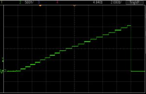
It's a 12bit ADC, set up to sample 2 channels. It is pretty precise, it's maximum value is 2.048 V, and it clips at pretty much that exact value. The overall linearity is surprisingly high. Guess, we've come a long way with micros these days. There's an ADC monitor mode (command ~M), which reads both ADC channels every 50ms. It's only useful when used in a terminal.
DAC – Pins 4.0 (DAC1) & 5.0 (DAC2) also pin 5.2 (DAC 2 Buffered)
DACs are 8bit current DACs. That means the input value is translated into a current rather than a voltage. A resistor is needed to turn the current into a voltage. The maximum output current is 612µA. A good choice would be 4.2k so that the end value translates roughly to 2.55 Volts which is about 10mV per bit. The exact value would be 4.17k. If you get really bad 4.3k resistors, maybe salvaged, there might be a 4.2k or even 4.17k amongst them. Or you just use a trimmer pot. The specified current value for the DAC is 2.4µA per bit.
In addition to the regular output, DAC 2 is internally connected to an op-amp. If the op-amp is switched on, it buffers the voltage on the output of DAC 2 with a gain of 1 and outputs it on pin 5.2. For this to work a resistor is needed from pin 5.0 to GND. (See previous paragraph)
The polarity of both DACs can be set to positive or negative. If it's set to positive the DAC sources current towards GND. If it's set to negative it sinks current from VDD.
I²C Interface – Pins 7.0 (SCL) & 7.1 (SDA)
Sending and receiving I²C data is a bit more involved due to the "complexity" of the interface. Since I²C is used by tons if different peripheral devices, I tried to make the protocol as flexible as possible.
The protocol consists of a series of data bytes (two hex digits) and separators (a single character). Multiple data bytes can be combined to form a complete interaction with a I²C device.
The following image shows a transaction between the GPIO and a serial EEPROM memory chip. First the device address with the R/W bit=0 (write) is sent, then two bytes with the memory address are sent, each followed by an ACK from the slave. After that a “Restart” condition is sent, followed by the device address again, this time the R/W bit is 1 (read). After the ACK from the slave, the master continues to clock to read data from the I²C memory. In this case, the value 0x42 (0100 0010) is read. After that a NOACK is sent by the master to inform the slave that no further data will be read.
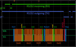
ga0+12+34+a1s00r
Which means: 'g' : start I²C command, 'a0' : device address with R/W bit 0, '+' : more bytes to come, '12' : high byte of the memory address, '+' : same, '34' : low byte, 'a1' : device address with R/W bit 1, 's' : insert a restart before sending 'a1′, '00' : dummy byte to create clock pulses for reading, 'r' : read data during dummy byte. Because the last byte is data that's sent by the memory device, the dummy byte ('00') is ignored and the value 0x42 is placed on the bus by the memory. The 'r' also terminates the transaction with the device by sending a NOACK and a "Stop" condition. It also terminates the I²C command sequence for the GPIO. For detailed information on the protocol read the section about SPI. Differences to SPI: There's no 'p' or 'P'. Instead of a pause, I²C uses the restart condition which is inserted via 's' (see above). The 'r' and 'R' separators send NOACK and ACK respectively.
SPI Interface – Pins 4.0 (MOSI), 4.1 (MISO), 4.2 (CLK), 4.3 (CS)
The SPI interface works just like I²C. So here are some more details about the protocol.
Except for the initial prefix 'e' for SPI commands or 'g' for I²C the protocol is suffix controlled. That means that the separator acts on the preceeding byte. In the command: ga1+12R34r, the 'R' means “read a byte while writing a 0x12. Bytes written during reads are usually dummy bytes to creates clock cycles. So their value doesn't matter. However, some SPI devices might read and write at the same time.
The available separators are:
- + = more bytes follow
- r = read byte and terminate message
- R = read byte but don't terminate
- p = insert pause, by deactivating CS for 10µs
- P = insert pause and read
- . = terminate message
The separators '+', 'p', 'P' and 'R' always expect another byte. There's a certain limit on how many commands can be sent in a single message. This depends on the BAUD rate, the type of command and the device. I highly recommend to hook up an osci to get a look at the relationship between the RS232 data and the SPI message (or I²C) to determine if the commands work properly.
In the following examples I assume device address 0x50 and the read/write bit is bit 0 (LSB).
e50+01+f0.
'e' initiates an SPI message. 1st, the device address with R/W=0 (write) is sent, followed by two bytes. '.' terminates the message and the firmware returns to idle state.
1st example: e51+00r / 2nd example: e51+00R00r
Here the device address is sent with R/W=1 (read), hence 0x51. The 1st example reads one byte, the second example reads two bytes. All 0x00 are dummy bytes to create clock cycles.
e50+aa+55p51+00R00R00r
1st byte (device address) with R/W=0 again (write), then two bytes
0xaa and 0x55 are sent. After that the CS signal is deactivated using
the separator 'p'. 10 microseconds later CS is activated again and the
device address with R/W=1 is sent to then read three bytes in a row (00R00R00r).
It depends on the CS polarity if CS is raised or lowered during the
pause. The same access to the device could be done in two separate
commands:
1st: e50+aa+55.
followed by: e51+00R00R00r
Note that a message can be cancelled using [ESC] when a separator is excpected, or '.' when a byte is expected.
Pulse Generator – Pin 3.7
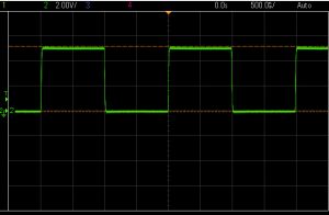
There's not much to tell about the pulse generator. It has two input clock settings (1 kHz or 1 MHz) in order to get the wide frequency range. After playing around with it, I discovered a few downsides of the simple timer/flipflop arrangement – mainly jitter. From a frequency perspective it get's quite coarse at the upper end. Top is 500kHz, one bit down: 330 kHz, -1 again => 250 kHz, you get the idea. It only feels linear if you think in seconds (milli/micro).
Cyclic Readout, Egde Trigger and External Trigger – Pin 3.6 (Ext. Trigger)
Automatic data readout can be triggered by either a timer, a change of value on one of the ports or by an external trigger. See the command listing for details on how to use it.
The Edge triggering can be configured for each pin individually. Edge triggering also triggers the IO monitor (command 'M').
Cyclic readout can be activated in steps of 1 ms, up to 65535 ms. However, the minimum interval depends on the BAUD rate settings and the type of data that's sent. I made a test at 115200 BAUD, the minimum interval was 2ms when reading out the word with full timestamp and '\r\n' as separator. When just reading out the word value, I got down to 1ms interval.
RS232 and User Interface – Pins 1.0 (Rx) & 1.1 (Tx)
No magic happens around the RS232 interface. It's standard TTL level. The common – nay ubiquitous – FTDI TTL232-to-USB converters will work fine. I designed the command syntax so that it's quite efficient for fast interaction with the IO peripherals. It's not so much designed for interaction with a human. It's primarily meant to be used via a software that runs on a PC, a µC or an embedded system. That's why the default number-base is hexadecimal. Hex letters are always lower case (abcdef). The output can be switched to upper case hex letters or to decimal . Whenever useful multiple bases are displayed.
Decimal Input
There are some commands that allow decimal input. It follows the
reverse input notation. Means, the number is entered and then followed
by the command character, like: 123h to set the high byte to 123(dec). Or you enter 12345w to set the whole word to 12345(dec), which would be equivalent to typing: w3039
Number digits have to be entered consecutively, any other character will
reset the input buffer. There are only a few commands that support
decimal input:
l, h, w, a, o, x, A, O, X, s, z, P, L, ~a, ~b
To make it easier to work with hex numbers, there's a dec->hex converter built in, command: '#'.

The Commands
Commands are case sensitive! Due to the fact that the feature list got a little out of hand I had to cramp many commands into the software, in a somewhat sensible way, just using ASCII. So the command for reading the port value as a word (16bit) became 'D' as in dump, because 'w' and 'W' were used for other functions. "Clear word" became 'F' for "flush" and so on.
Commands are not terminated. That means for hex input, after the last digit is typed the value is used by the given command routine. After typing P12ab the pulse generator immediately jumps to 4779 ms period.
The same goes for decimal input the number is terminated by the command character, but the command itself is not terminated any further. You type: 123~a – bam – DAC 1 changes its value (if it's not at 123(dec), already, duh).
It might be easier to work with the IO board when echoing is activated '*X01'
This is the list of all available commands:
<nn>   = one HEX byte (lower case letters !!)
<nnnn> = two HEX bytes (one HEX word)
-------------------------------
l<nn>    - set low byte (port 0)
h<nn>    - set high byte (port 2)
w<nnnn>  - set word
a<nn>    - port AND byte -> port
o<nn>    - port OR byte -> port
x<nn>    - port XOR byte -> port
A<nnnn>  - port AND word -> port
O<nnnn>  - port OR word -> port
X<nnnn>  - port XOR word -> port
c        - clear low byte
C        - clear high byte
F        - clear word (flush)
s<n>     - set bit, bit number as one hex digit (0..f)
z<n>     - clear bit (zero)
i        - invert low byte
I        - invert high byte
N        - invert word (negate)
r        - read low byte; returns 2 HEX digits "hh"
R        - read high byte
D        - read word (dump); returns 4 HEX digits "hhhh" (MSB left)
S        - read ADC value (pin 1.4 & 1.5), result depends on *X4
P<nnnn>  - set pulse generator period, 0000 disables pulse generator
L<nnnn>  - set pulse width (length) !! Pulse Generator on Pin 3.7 !!
M        - PIO monitor on/off (edge triggered)
[SPACE]  - show register status
?        - this help page
#        - convert decimal number to hex
.        - cancel transmission, acknowledged by '#'
[ESC]    - cancels all automatic readouts (kinda buggy)
b<nn><...> - send low byte burst, <nn> is number of bytes in burst
             <...> = 2byte hex values, no separator: b<nn><d0><d1>...<dn>
B<nn><...> - send high byte burst; bursted data is not cached
W<nn><...> - send word burst, <nn> is number of words (4byte hex value)
-------------------------------
~a<nn>   - set value for DAC 1 (pin 4.0)
~b<nn>   - set value for DAC 2 (pin 5.0, buffered on 5.2 (see *?)
~P<nn>   - set DAC polarity; 0=negative (sink), 1=positive (source)
           each digit for one DAC: <ab>, (<10> -> (DAC1+, DAC2-))
~r<nnnn> - read ADC value repeatedly every <nnnn> msec
~M       - monitor ADCs (pin 1.4 & 1.5) (50ms Interval)
-------------------------------
*D<nnnn> - set pin direction (1=in, 0=out; default 0xffff)
*O<nnnn> - set output type (0=totem-pole, 1=open drain; default 0000)
*P<nnnn> - enable strong pull-up (~5k, can drive LEDs),
           0=off, 1=on, default 0000, ignored if output is totem-pole
*L<nnnn> - LED mode (can also be used as input to read simple switches)
           overrides all other port settings! 0=on, 1=off, default 0000
*T<nnnn> - trigger readout on rising edge @ specific pin,
           0=trigger off, 1=trigger readout
*t<nnnn> - trigger readout on falling edge @ specific pin
*r<nnnn> - read low byte repeatedly every <nnnn> msec,
           0000 disables repetitive readout
*R<nnnn> - read high byte repeatedly
*W<nnnn> - read word repeatedly
*B<x>    - boolean byte function for:
           x==0 -> low byte (default) / x!=0 -> high byte
*E<nnnn> - enable external triggering (pin 3.6)
           <nnnn> means: <*eda> -> e(egde), d(digital), a(adc)
           trigger edge,    e: 0=off,  1=rising, 2=falling, 3=both
           digital readout, d: 0=none, 1=low, 2=high, 3=word
           analog readout,  a: 0=none, 1=adc1, 2=adc2, 3=adc1:adc2
*?       - paged help page & some extra information
*V       - get FW version; answer: "!<version>"
*p       - ping; answer: "!PONG"
*Y42     - reset device
*Y99     - restore factory settings (*X<x> settings), requires reset
*C       - read config, format:
           !<Version>,<DReg><DCache>,<P>,<L>,<*D>,<*O>,<*P>,<*L>,
           <*T>,<*t>,<~a>,<~b>,<~P>,<*B>,<*X0>,<*X1>,<*X2>,<*X3>,<*X4>,
           <*X5>,<*X6>,<*X7>,<*X8>,<*X9>\r\n
             <DReg>   = port data register (output latch, not pin state)
             <DCache> = port data cache (last value written)
------------------------------
system config commands: (will be stored nonvolatile)
*X0<x>   - console echo; x==0 -> off; x!=0 -> on
*X1<x>   - append line break or separator after read
           x: 0=off 1=\n 2=\r 3=\r\n 4=' ' 5=, 6=; 7=/ 8=Tab
*X2<x>   - set BAUD rate: x: 0=2400, 1=4800, 2=9600, 3=19200, 4=38400,
                             5=57600 (default), 6=115200, 7=230400
*X3<x>   - case of hex letters; x: 0=lower case, 1=upper case
*X4<x>   - set channel for ADC readout; x: 0=Ch1, 1=Ch2, 2=Ch1 & Ch2
           output on dual-channel: <nnnn>:<mmmm> (n=ch1, m=ch2)
*X5<x>   - edge triggered readout; x: 0=word, 1=low byte, 2=high byte
*X6<x>   - pulse generator main clock frequency; x: 0=1MHz (default), 1=1kHz
*X7<x>   - timestamp format; x: 0=no timestamp, 1='HHMMSS-', 2='MMDD.HHMMSS-'
           NOTE: lowers performance, always starts at 01.01.1970/00:00:00
*X8<x>   - default readout base: x: 0=HEX (default), 1=DEC
*X9<x>   - enable opamp; x: 0=disabled (default), 1=enabled (pin 5.2)
Note! For the sake of efficiency, there's no error detection on entering values. So, typing things like 'w03xy' (where the number is partly invalid in this example), will result in whatever. The firmware might even crash (yes, that's how lazy I am). But, commands can be cancelled at any time by typing '.' . Decimal input will overflow at 65535. The resulting value is usually useless but will always be a valid integer.
How to Use from the Command Line
On Windows the module can be controlled via the command 'echo'. To set the BAUD rate of the COM port use:
mode COMx BAUD=57600 PARITY=N DATA=8 STOP=1 xon=off
Replace 'COMx' with the COM port on your computer.
To send commands to the PIO module use:
echo h1c > COMx
That sets the high byte to 1c(hex)/28(dec).
Multiple commands can be sent at once:
echo *Dff00*O00ff*Pffff0l200~a~bff > COMx
Means: "low byte output, high byte input"[*Dff00], "low byte output type: open drain"[*O00ff], "all pull-ups on"[*Pffff], "set low byte to 0″[0l], "set DAC 1 to 200(dec)"[200~a], "set DAC 2 to ff(hex)"[~bff].
Software
The software was developed using Cypresses 'PSoC Creator 4.2'. Link to the project files for the GPIO below. There's not much to do, except for building the project and programming it into the device.
Note that after programming the board, the BAUD rate is always set to 57600 8N1. That's due to the way the flash memory is used to emulate an EEPROM.
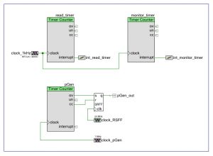
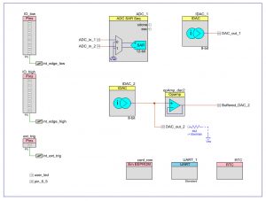
Here's a view at the peripheral configuration. Never had thought I would end up needing two pages.
- PSoc Creator project files: GPIO232_16
Other Stuff
I made a set of labels to put on rows of pin sockets on either side of the board.
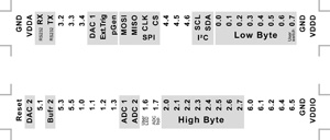
There’s also a PDF Version in the software package.
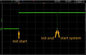
The LED on top of the board shows when an input is recognized by toggling on and off. During startup, this LED sends an init-pulse, means that it switches on at the beginning of the init routine and off after the complete init of the controller. After that it switches on again to indicate "power on". The LED is connected to pin 1.6. This pulse sequence is only visible using an oscilloscope. It's meant for diagnosis.
Known Bugs / Missing Features
- Cancelling automatic readouts or monitor modes by [ESC], sometimes crashes the firmware.
- The clock cannot be set, so the timestamps aren't really timestamps. It's more like relative markers of time passed.
- Some of the automatic readouts can interfere with each other, especially egde triggering and external triggering.
- The IO monitor loses trigger events if they occur too fast.
- The pulse generator is quite jittery, which might be caused by timing interference between the timer clock and the flip-flop clock (yes, flip-flops are clocked in this controller (internal syncronisation purposes)).
- The long version of the status screen cannot be displayed in pages.
- There's some crosstalk between the ADC channels. Got no numbers on that.
- In most cases when the firmware crashes the reset command (*Y42) will not work either.
- There's no way to change the BAUD rate without using the the commands. If you have locked yourself out of the device by setting the wrong BAUD rate, you have to change the settings of the COM port you're using to be able to talk to the PIO again.
- There are a few more output driver modes that can't be used by the software.
- The ADC could technically read more than two channels, but configuring many channels through the UI would be a nightmare. There are also two unused 7bit DACs.
- One of the remaining three op-amps could be made available to the user for general use.
- A function to shift and roll data through the bytes/word would be neat.
- Using all the unused pins as inputs with just simple direct readout.
Conclusion
This is probably the most finished project on this page.
Comments
